Search Constraints
Search Results
Select an image to start the slideshow
電子分光法における表面感度と検出深さ
1 of 16
Inelastic Scattering of Electrons in Solids
2 of 16
表面電子分光法における信号の減衰は如何に記述されるか? IV. 単位系,平均自由行程, 一般化振動子強度
3 of 16
“Word”で数式をきれいに記述するには
4 of 16
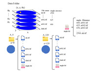
Sample data for X-ray visualization of local bending of the lattice planes (XR-V-LBLP)
5 of 16
電子分光法における表面定量分析の標準化の歩み
6 of 16
Analysis of electron inelastic scattering in solids over wide energy range and its application to surface chemical analysis
7 of 16
Electron Inelastic Mean Free Paths in Liquid Water for Energies from10 eV to 10 keV
8 of 16
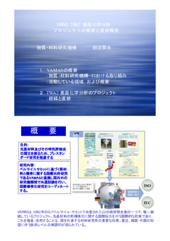
TWA2 表面分析化学 2005年度のプロジェクトの概要と進捗
9 of 16
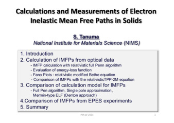
Calculations and Measurements of Electron Inelastic Mean Free Paths in Solids
10 of 16
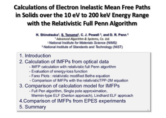
Calculations of Electron Inelastic Mean Free Paths in Solids over the 10 eV to 200 keV Energy Range with the Relativistic Full Penn Algorithm
11 of 16
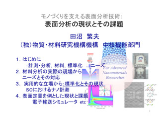
モノづくりを支える表面分析技術: 表面分析の現状とその課題
12 of 16
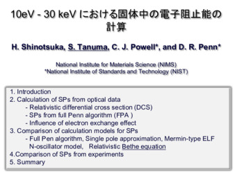
10eV - 30 keVにおける固体中の電子阻止能の計算
13 of 16
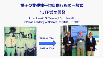
電子の非弾性平均自由行程の一般式:JTP 式の開発
14 of 16
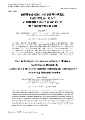
表面電子分光法における信号の減衰は如何に記述されるか? V. 誘電関数を用いた固体における電子の非弾性散乱断面積
15 of 16

XPS spectral data for p- and n-type Si wafers with various resistivities acquired at SPring-8 BL15
16 of 16