Search Constraints
Search Results
Select an image to start the slideshow
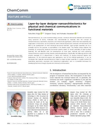
Layer-by-layer designer nanoarchitectonics for physical and chemical communications in functional materials
1 of 9
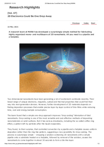
[Research Highlights Vol.67] 2D Electronics Could Be One Drop Away
2 of 9
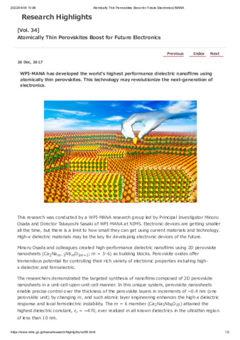
[Research Highlights Vol.34] Atomically Thin Perovskites Boost for Future Electronics
3 of 9
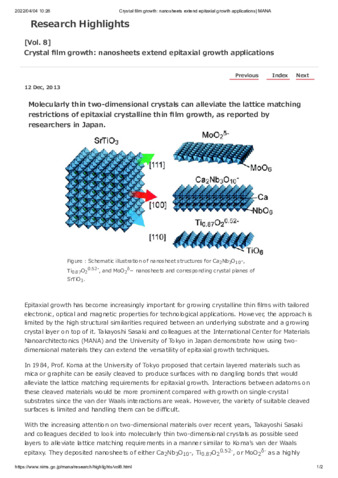
[Research Highlights Vol.8] Crystal film growth: nanosheets extend epitaxial growth applications
4 of 9
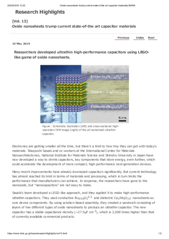
[Research Highlights Vol.13] Oxide nanosheets trump current state-of-the art capacitor materials
5 of 9
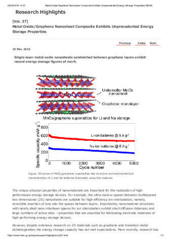
[Research Highlights Vol.37] Metal Oxide/Graphene Nanosheet Composite Exhibits Unprecedented Energy Storage Properties
6 of 9
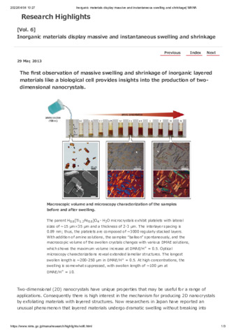
[Research Highlights Vol.6] Inorganic materials display massive and instantaneous swelling and shrinkage
7 of 9
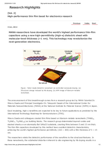
[Research Highlights Vol.2] High-Performance Thin Film Boost for Electronics Research
8 of 9
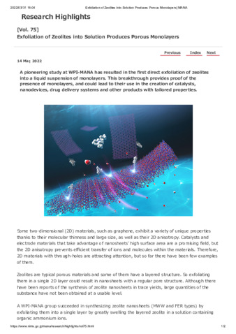
[Research Highlights Vol.75] Exfoliation of Zeolites into Solution Produces Porous Monolayers
9 of 9