Search Constraints
« Previous |
21 - 30 of 57
|
Next »
Search Results
Select an image to start the slideshow
表面電子分光法における信号の減衰は如何に記述されるか? V. 誘電関数を用いた固体における電子の非弾性散乱断面積
1 of 10
Calculations of Electron Inelastic Mean Free Paths III. Data for 15 Inorganic compounds over the 50 - 2000 eV Range
2 of 10
Calculations of Electron Inelastic Mean Free Paths II. Data for 27 Elements over the 50 - 2000 eV Range
3 of 10
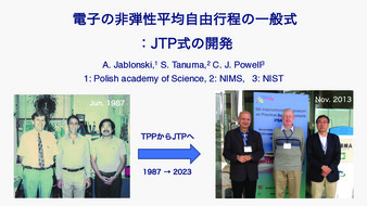
電子の非弾性平均自由行程の一般式:JTP 式の開発
4 of 10
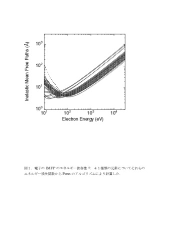
Determination of Inelastic Mean Free Paths in Elemental Solids in the 200 to 5000 eV Energy Range by Absolute Elastic Peak Electron Spectroscopy
5 of 10
表面電子分光法における電子の散乱効果の研究
6 of 10
Structuring Superconductor Data with Ontology: Reproducing Historical Datasets as Knowledge
7 of 10
10eV - 30 keVにおける固体中の電子阻止能の計算
8 of 10
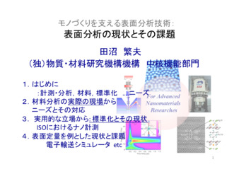
モノづくりを支える表面分析技術: 表面分析の現状とその課題
9 of 10
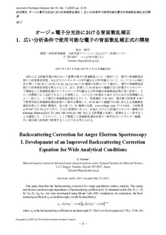
オージェ電子分光法における背面散乱補正 I.広い分析条件で使用可能な電子の背面散乱補正式の開発
10 of 10